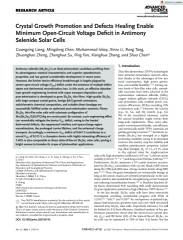
Crystal Growth Promotion and Defects Healing Enable Minimum Open-Circuit Voltage Deficit in Antimony Selenide Solar Cells
Résumé
Antimony selenide (Sb(2) Se(3) ) is an ideal photovoltaic candidate profiting from its advantageous material characteristics and superior optoelectronic properties, and has gained considerable development in recent years. However, the further device efficiency breakthrough is largely plagued by severe open-circuit voltage (V(OC) ) deficit under the existence of multiple defect states and detrimental recombination loss. In this work, an effective absorber layer growth engineering involved with vapor transport deposition and post-selenization is developed to grow Sb(2) Se(3) thin films. High-quality Sb(2) Se(3) with large compact crystal grains, benign [hk1] growth orientation, stoichiometric chemical composition, and suitable direct bandgap are successfully fulfilled under an optimized post-selenization scenario. Planar Sb(2) Se(3) thin-film solar cells with substrate configuration of Mo/Sb(2) Se(3) /CdS/ITO/Ag are constructed. By contrast, such engineering effort can remarkably mitigate the device V(OC) deficit, owing to the healed detrimental defects, the suppressed interface and space-charge region recombination, the prolonged carrier lifetime, and the enhanced charge transport. Accordingly, a minimum V(OC) deficit of 0.647 V contributes to a record V(OC) of 0.513 V, a champion device with highly interesting efficiency of 7.40% is also comparable to those state-of-the-art Sb(2) Se(3) solar cells, paving a bright avenue to broaden its scope of photovoltaic applications.
Fichier principal
 Liang - Crystal Growth Promotion and Defects Healing Enable Minimum Open%u2010Circuit Voltage Deficit.pdf (5.11 Mo)
Télécharger le fichier
Liang.pdf (1.66 Mo)
Télécharger le fichier
| Origine | Fichiers éditeurs autorisés sur une archive ouverte |
|---|

